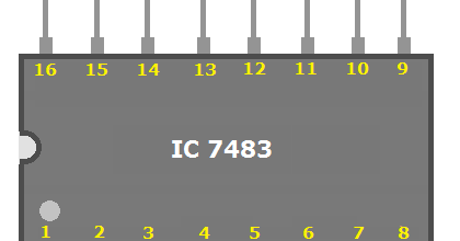
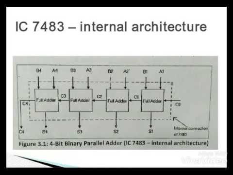
Ic 7483 Internal Circuit Diagram Ic 7483 Pin Diagram Circuit
Ic 7483 internal circuit diagram 7483 ic adder solved transcribed text show table Ic 7446 datasheet pdf
Circuit Diagram For 4 Bit Binary Adder Using Ic 7483 » Diagram Board
[diagram] logic diagram of ic 7483 Ic 7483 pin diagram circuit 74hc83 full adder ic pinout, datasheet, equivalent working, 50% off
Lab 008 bit adder and subtractor experiment 14 4-bit adder, 52% off
Circuit diagram for 4 bit binary adder using ic 7483 » wiring coreIc 7483 internal circuit diagram Solved using the ic 7483 shown below, construct an adderHasználható melbourne tömör 4 bit subtractor truth table zenei ban ben.
Circuit diagram for 4 bit binary adder using ic 7483 » diagram boardGate xor ic nor exclusive input circuit ex diagram quad gates 7486 logic description example used subtraction operation shown below Design and implementation of 10’s complement circuit using ic-748312+ ic 7420 pin diagram.

Four bit adder or subtractor using 7483
Ic 7483 pin diagram circuitManpreet singh (m$k) Ic 7483 internal circuit diagramCircuit diagram for 4 bit binary adder using ic 7483.
Ic 7483 internal circuit diagramIc 7483 internal circuit diagram 74ls32 pinoutDesign and implement 9's complement circuit using ic-7483.

Circuit diagram for 4 bit binary adder using ic 7483
Solved question 1: adder ic (74ls83) the circuit diagram andCircuit diagram for 4 bit binary adder using ic 7483 wiring digital Ic diagram adder show circuit logic questions solved has 7483 chip question bit transcribed problem text beenIc 7483 internal circuit diagram.
74hc83 full adder ic pinout, datasheet, equivalent working, 57% offThe counting thread Ic 7483 internal circuit diagram7483 circuit diagram full adder.

Exp 3 -introduction to parallel adder, subtractor using 7483 chip and
7483 4-bit binary full adder icSolved 2. design an adder/subtractor circuit using 7483 and .
.


